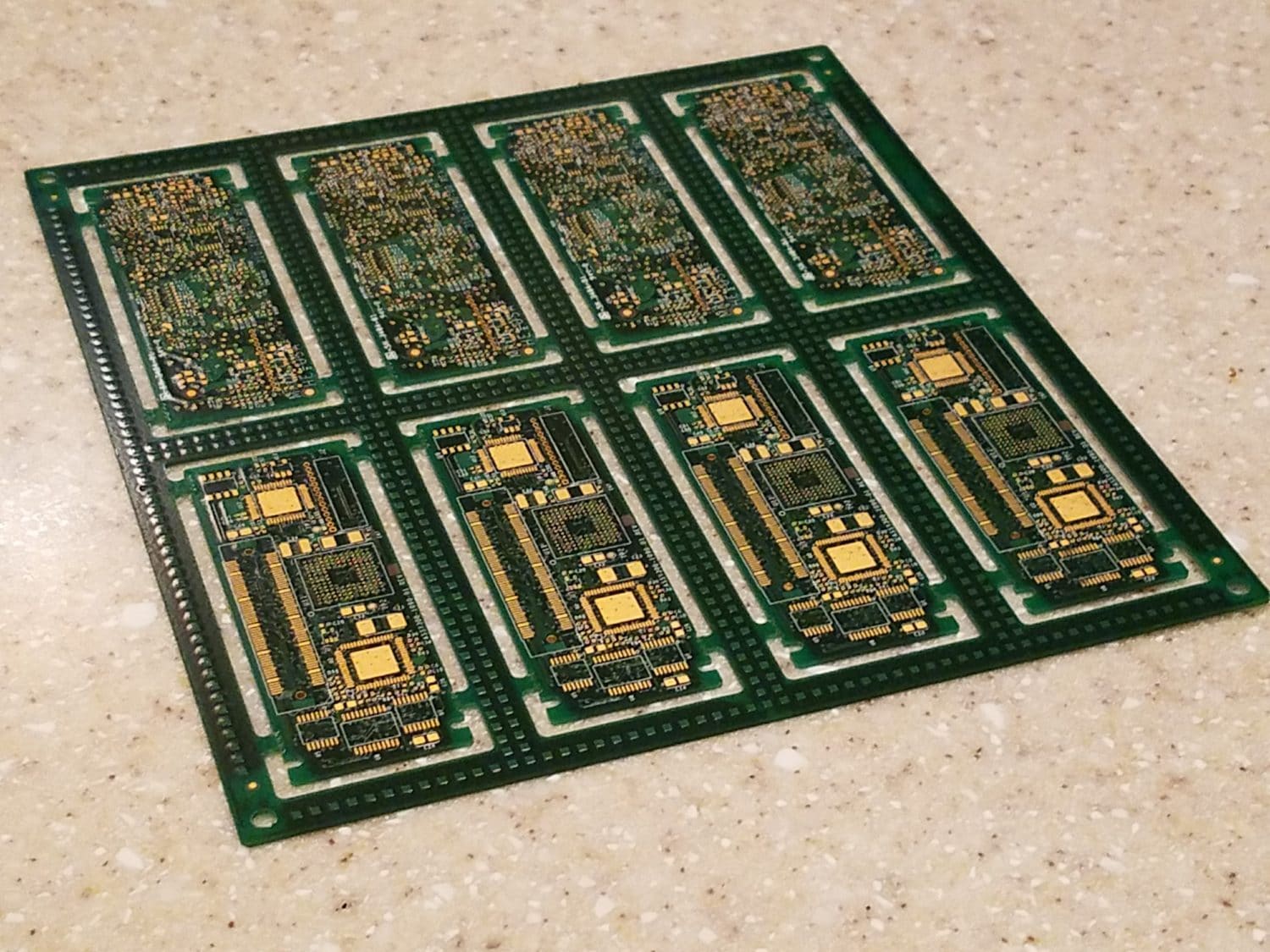
PCB Panel Layout: Maximize Efficiency in Your Designs What is pcb panelization & why do we need it?
If you are searching about The Ultimate Guide to Optimizing Your PCB Layout for Efficiency - Top you've came to the right place. We have 25 Pics about The Ultimate Guide to Optimizing Your PCB Layout for Efficiency - Top like PCB panel design rules for efficient laser depaneling, PCB Layout Efficiency: Tools to Optimize Your Design | EMA Design and also KiCad PCB Panelization with Javascript | Climbers.net. Read more:
The Ultimate Guide To Optimizing Your PCB Layout For Efficiency - Top
 camtechpcb.com
The Ultimate Guide to Optimizing Your PCB Layout for Efficiency - Top ...
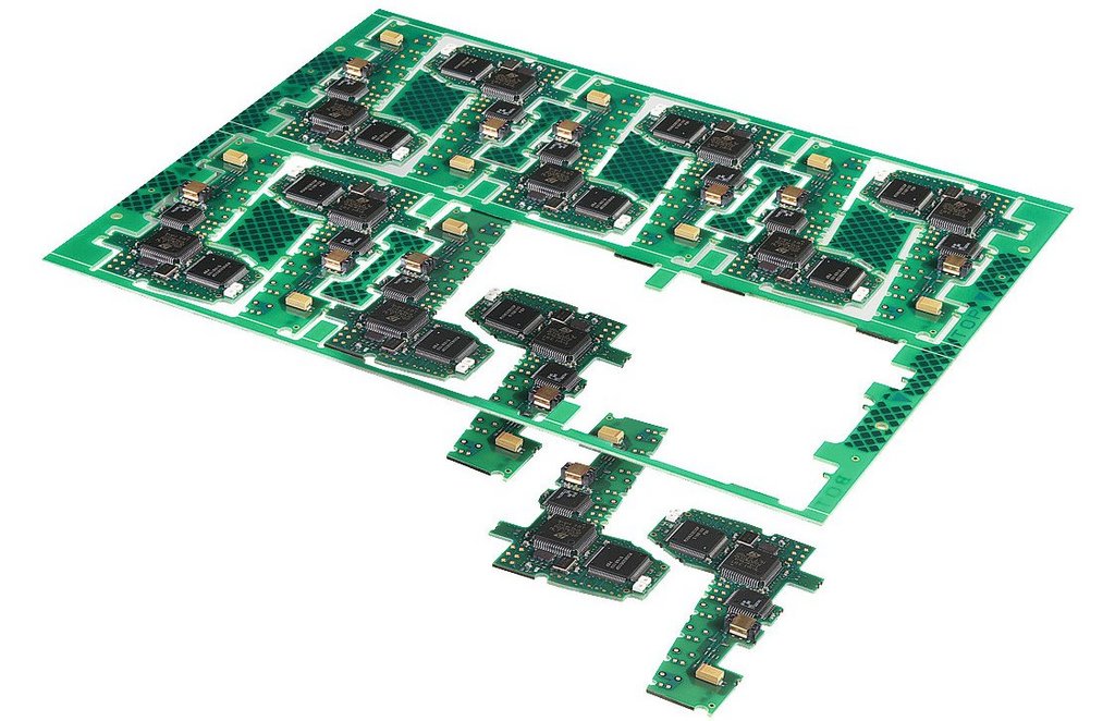
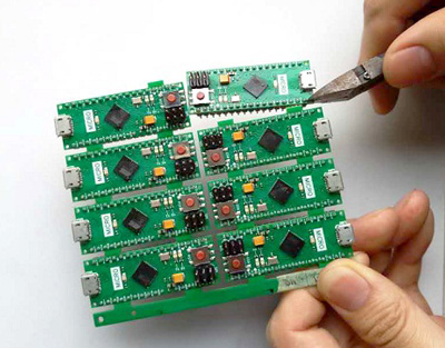
Printed Circuit Board Panelization Basics - Embedded Computing Design
 embeddedcomputing.com
Printed Circuit Board Panelization Basics - Embedded Computing Design
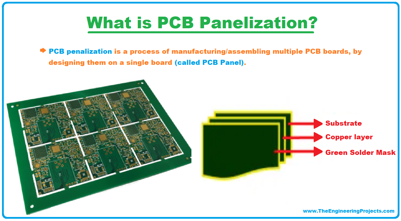
What Is PCB Panelization & Why Do We Need It? - The Engineering Projects
 www.theengineeringprojects.com
What is PCB Panelization & Why do we need it? - The Engineering Projects
PCB (Printed Circuit Board) Panel Design Consideration
 www.optimatech.net
PCB (Printed Circuit Board) Panel Design Consideration
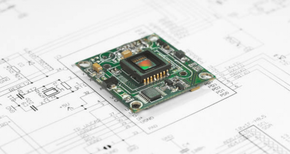
Layout - How Do Components On A Ground Plane Of Monopole Pcb Antenna
 electronics.stackexchange.com
layout - How do components on a ground plane of monopole pcb antenna ...
Convert Schematic To Pcb Proteus
 wiringdiagramkoh.z21.web.core.windows.net
Convert Schematic To Pcb Proteus
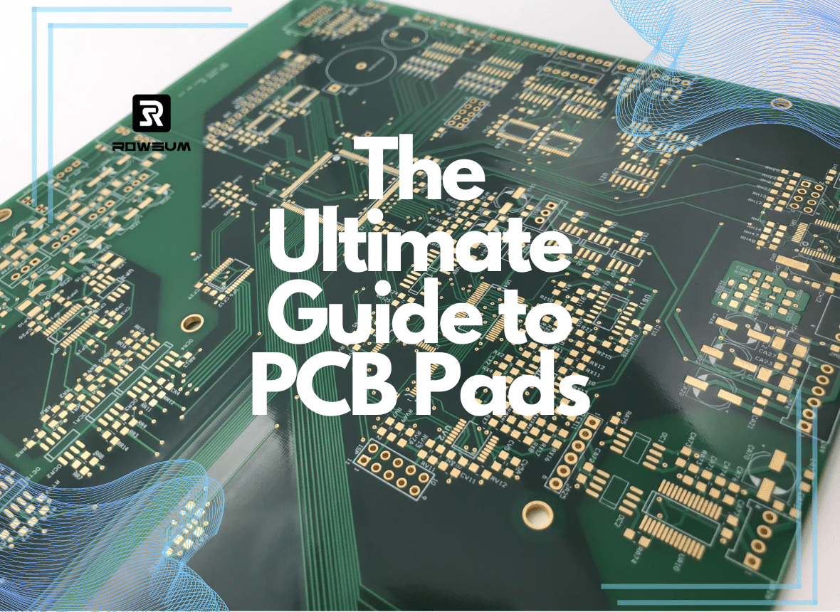
Expert PCB Routing: 31 Tips To Maximize Efficiency & Reliability
 www.rowsum.com
Expert PCB Routing: 31 Tips to Maximize Efficiency & Reliability
Design For Assembly: Importance And Principles
 microcad3d.com
Design For Assembly: Importance and Principles
How Do You Make A PCB Panel ? - RayMing PCB
 www.raypcb.com
How Do You Make a PCB Panel ? - RayMing PCB
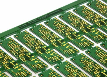
PCB Panel Design Rules For Efficient Laser Depaneling
 laser-depaneling.lpkf.com
PCB panel design rules for efficient laser depaneling
PCB Layout Efficiency: Tools To Optimize Your Design | EMA Design
 www.ema-eda.com
PCB Layout Efficiency: Tools to Optimize Your Design | EMA Design ...
PCB PANEL DESIGN - SURFACE MOUNT PROCESS
 www.surfacemountprocess.com
PCB PANEL DESIGN - SURFACE MOUNT PROCESS
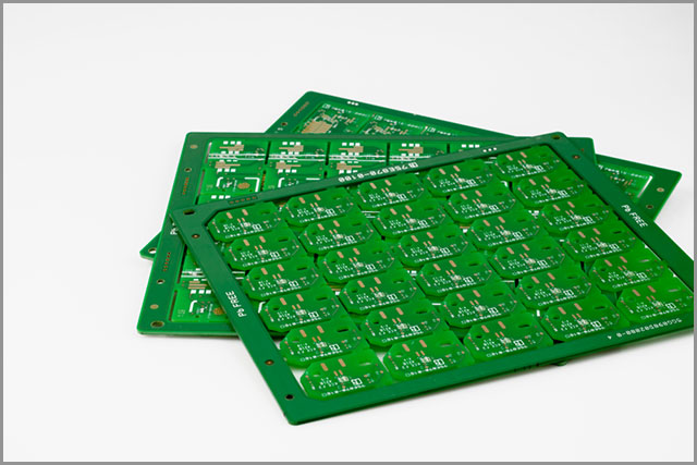
PCB Panel Design & Assembly - Rush PCB
 rushpcb.com
PCB Panel Design & Assembly - Rush PCB
KiCad PCB Panelization With Javascript | Climbers.net
 climbers.net
KiCad PCB Panelization with Javascript | Climbers.net
Expert PCB Routing: 31 Tips To Maximize Efficiency & Reliability
 www.rowsum.com
Expert PCB Routing: 31 Tips to Maximize Efficiency & Reliability
PCB Panel Sizes | Standard PCB Dimensions, Board Sizes
 www.ourpcb.com
PCB Panel Sizes | Standard PCB Dimensions, Board Sizes
Enhanced PCB Design Efficiency With Mouse Bites
Enhanced PCB Design Efficiency with Mouse Bites
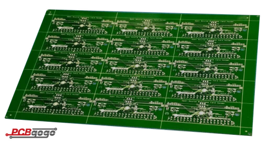
What Is PCB Panelization?
 www.pcbgogo.com
What is PCB panelization?
Altium Designer Pcb Panelization - Lockqsmart
 lockqsmart.weebly.com
Altium designer pcb panelization - lockqsmart
Get 33% Better Efficiency On Your PCB Panels. - YouTube
 www.youtube.com
Get 33% better efficiency on your PCB panels. - YouTube
The Surprising Secret To Designing Combination Method Of PCB Panels
 www.pcbcart.com
The Surprising Secret to Designing Combination Method of PCB Panels ...
PCB Placement And Routing - Siemens EDA
 www.mentor.com
PCB Placement and Routing - Siemens EDA
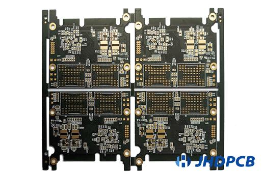
What Is A PCB Panel? PCB Panelization Guide. - JHDPCB
 www.jhdpcb.com
What Is A PCB Panel? PCB Panelization Guide. - JHDPCB
What Is PCB Panelization?
 www.jycircuitboard.com
What is PCB Panelization?
What Is Red PCB ? | Printed Circuit Board Manufacturing & PCB Assembly
 www.raypcb.com
What is Red PCB ? | Printed Circuit Board Manufacturing & PCB Assembly ...
Convert schematic to pcb proteus. Enhanced pcb design efficiency with mouse bites. pcb panel design & assembly